From PCB board to 3D model or mesh
A circuit board goes to mechanical CAD as a 3D model, to fit its enclosure, and to a field solver as a mesh of its copper. planex2d reads the board with every copper layer named by net, builds the whole board in 3D from its stackup, writes it as STEP, and passes the copper of one net to netgen. KiCad boards are read directly, and boards from Altium, Eagle, PADS, EasyEDA, CADSTAR, Fabmaster, P-CAD, gEDA, Cadence Allegro and SolidWorks PCB through KiCad 10’s kicad-cli. The first cell is the
complete workflow, ready to copy and run, and the section Step by step runs it in parts, with the plots one looks at along the way.
The example is the pic_programmer demo from KiCad’s own demo projects, demos/pic_programmer in the KiCad repository, licensed CC BY-SA 4.0 by the KiCad project. The pictures on this page made from it are under the same license. The board file is pic_programmer.kicad_pcb.
[2]:
import ngsolve as ngs
from ngsolve_webgpu.jupyter import Draw
import planex as px

board = px.FromKiCad("pic_programmer.kicad_pcb")
area = {}
for f in board["B.Cu"].faces:
    area[f.name] = area.get(f.name, 0.0) + f.mass
print("largest nets on B.Cu", sorted(area.items(), key=lambda kv: -kv[1])[:3])
gnd = px.Unify(list(board["B.Cu"].faces(name="GND")))

model = px.FromKiCad("pic_programmer.kicad_pcb", px.stackups.kicad)
model.WriteStep("pic_programmer.step")

gnd.name = "GND"
mesh = ngs.Mesh(px.OCCGeometry(gnd).GenerateMesh(maxh=0.002))
print(mesh.ne, "elements |", mesh.GetMaterials())
Draw(mesh)
PlanexWarning: FromKiCad: 223 texts left out (not supported yet)
largest nets on B.Cu [('GND', 0.010673650980717526), ('/pic_sockets/VCC_PIC', 0.00013793475583072988), ('/VPP/MCLR', 0.00013182877907773092)]
PlanexWarning: FromKiCad: 19 texts left out (not supported yet)
82738 elements | ('GND',)
Step by step
Reading the board
px.FromKiCad returns one shape per layer, by KiCad’s layer names, in meters. The copper layers have their faces named by net and their drill holes cut out, and Edge.Cuts is the board’s outline as a face. The warning names what is not read yet, the texts. See KiCad for the layers and KiCad, Altium, Eagle and more for the boards of other programs.
[3]:
import ngsolve as ngs
from ngsolve_webgpu.jupyter import Draw
import planex as px

board = px.FromKiCad("pic_programmer.kicad_pcb")
print(list(board))
print("board", board["Edge.Cuts"].bounding_box)
['F.Cu', 'B.Cu', 'Edge.Cuts', 'F.SilkS', 'B.SilkS', 'F.Mask', 'B.Mask', 'Cmts.User', 'F.CrtYd', 'B.CrtYd', 'F.Fab']
board ((0.07366, -0.1397), (0.23368, -0.04064))
PlanexWarning: FromKiCad: 223 texts left out (not supported yet)
Finding a net
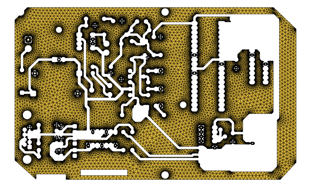
The faces of a copper layer carry their nets as names, so the copper of one net is a selection by name. Summed by net, the bottom layer’s largest copper is the ground pour, GND, far larger than any other net (Figure 1). px.Unify joins its faces into one region (see Boolean operations).
[4]:
area = {}
for f in board["B.Cu"].faces:
    area[f.name] = area.get(f.name, 0.0) + f.mass
print(sorted(area.items(), key=lambda kv: -kv[1])[:4])
gnd = px.Unify(list(board["B.Cu"].faces(name="GND")))
print("GND copper on B.Cu", gnd.mass)
# px.Plot(gnd)
[('GND', 0.010673650980717526), ('/pic_sockets/VCC_PIC', 0.00013793475583072988), ('/VPP/MCLR', 0.00013182877907773092), ('VCC', 0.00011995727191698253)]
GND copper on B.Cu 0.010673650980717526

The board in 3D
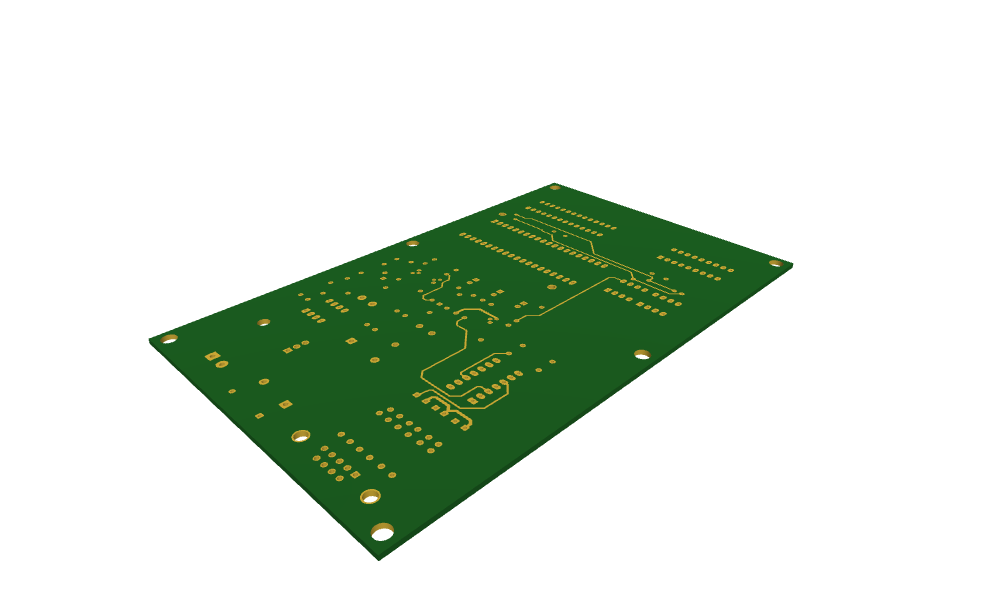
With a stackup instead of a layer name, px.FromKiCad returns the whole board as one OpenCASCADE shape, with the dielectric drilled through, the hole walls, and the copper layers at their heights, named by net. px.stackups.kicad takes the stackup stored in the board file, here a core of 1.51 mm, and px.stackups also holds manufacturers’ tables. WriteStep writes the model for the CAD program that designs the enclosure (see To OCC shapes).
[6]:
model = px.FromKiCad("pic_programmer.kicad_pcb", px.stackups.kicad)
print(len(model.solids), "solid,", len(model.faces), "faces")
model.WriteStep("pic_programmer.step")
Draw(model, settings={"Objects": {"Edges": False}})
PlanexWarning: FromKiCad: 19 texts left out (not supported yet)
1 solid, 713 faces
Meshing a net’s copper
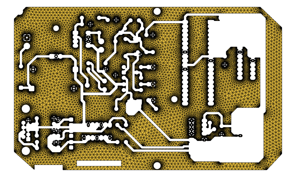
The ground pour’s name becomes the material of the mesh, and netgen meshes it with elements of at most 2 mm, ready for a field or current solve in NGSolve (see Meshing a face). gmsh takes the same face just as easily through WriteGeo (see gmsh and FEniCSx).
[7]:
gnd.name = "GND"
mesh = ngs.Mesh(px.OCCGeometry(gnd).GenerateMesh(maxh=0.002))
print(mesh.ne, "elements |", mesh.GetMaterials())
Draw(mesh)
82738 elements | ('GND',)
Other formats
Program |
Board file |
See |
|---|---|---|
KiCad |
|
|
Altium Designer |
|
|
Eagle |
|
|
EasyEDA |
|
|
PADS |
|
|
Allegro, CADSTAR, Fabmaster, P-CAD, gEDA, SolidWorks PCB |
Pitfalls
Units. The layers come in meters, so
maxh=0.002is 2 mm.Copper without thickness. In the 3D model, the copper layers are faces at their heights, without a thickness of their own. The dielectric carries the board’s thickness.
Boards from other programs. They need KiCad 10’s
kicad-cli, which fills their copper zones before reading. Without it, the call raises an error that names the missing tool.Large models. A board with many holes gives a model of many faces, and writing it as STEP takes OpenCASCADE a while.